| Sign In | Join Free | My burrillandco.com |
|
| Sign In | Join Free | My burrillandco.com |
|
| Ask Lasest Price | |
| Brand Name : | Bicheng |
| Model Number : | BIC-332.V1.0 |
| Certification : | UL, ISO9001, IATF16949 |
| Price : | USD9.99-99.99 |
| Payment Terms : | T/T |
| Supply Ability : | 5000PCS per month |
| Delivery Time : | 8-9 working days |
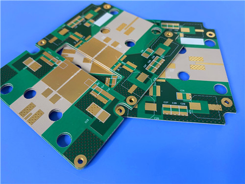
This 2-layer rigid PCB is tailored for high-frequency applications (exceeding 40 GHz), leveraging Rogers RO3203—a ceramic-filled, woven fiberglass-reinforced laminate—to deliver exceptional signal integrity, mechanical stability, and cost-effectiveness.
PCB Specification
| Parameter | Details |
| Base Material | Rogers RO3203 (ceramic-filled, woven fiberglass-reinforced PTFE composite) |
| Layer Count | 2-Layer (rigid structure) |
| Board Dimensions | 74.57mm x 23.28mm per piece (1PCS), |
| Minimum Trace/Space | 4 mils (trace) / 7 mils (space) |
| Minimum Hole Size | 0.2mm |
| Vias | No blind vias; via plating thickness = 20 μm |
| Finished Board Thickness | 0.35mm |
| Finished Copper Weight | 1oz (1.4 mils) for outer layers |
| Surface Finish | ENEPIG |
| Silkscreen | White silkscreen on top layer, no silkscreen on bottom layer |
| Solder Mask | Green solder mask on top layer, no solder mask on bottom layer |
| Quality Assurance | 100% electrical testing conducted prior to shipment |
PCB Stack-up Configuration
| Layer Name | Material | Thickness |
| Top Layer (Copper_layer_1) | 35 μm thick copper | 35 μm (1oz) |
| Substrate Layer | Rogers RO3203 | 0.254mm (10mil) |
| Bottom Layer (Copper_layer_2) | 35 μm thick copper | 35 μm (1oz) |
Rogers RO3203 Material Introduction
Rogers RO3203 is a premium high-frequency circuit material designed as an extension of the RO3000 Series, with a key focus on improved mechanical stability without compromising electrical performance. As a ceramic-filled laminate reinforced with woven fiberglass, it balances three critical attributes: exceptional electrical performance (suitable for frequencies beyond 40 GHz), robust mechanical stability, and competitive pricing—making it ideal for volume manufacturing of high-frequency devices.
Its core electrical properties—dielectric constant (Dk) of 3.02 and dissipation factor (DF) of 0.0016—enable reliable signal propagation at ultra-high frequencies, while its woven glass reinforcement ensures durability during handling and assembly. Unlike some high-frequency materials, RO3203 is also lead-free process compatible, aligning with global environmental standards.

RO3203 Key Features
The material’s features are tailored to meet the strict demands of ultra-high-frequency applications, combining electrical excellence with mechanical resilience:
| Feature | Specification |
| Material Composition | Ceramic-filled PTFE composite (woven fiberglass-reinforced) |
| Dielectric Constant (Dk) | 3.02 ± 0.04 at 10GHz/23°C |
| Dissipation Factor (DF) | 0.0016 at 10GHz/23°C |
| Decomposition Temperature (Td) | >500°C |
| Thermal Conductivity | 0.87 W/mK |
| Coefficient of Thermal Expansion (CTE) | X-axis: 13 ppm/°C; Y-axis: 13 ppm/°C; Z-axis: 58 ppm/°C (-55 to 288°C) |
| Process Compatibility | Lead-free process compatible |
| Flammability Rating | UL 94 V-0 |
Benefits
RO3203’s properties translate to tangible advantages for the PCB, addressing key challenges in ultra-high-frequency design and volume manufacturing:
Ultra-High-Frequency Performance: Low DF (0.0016) and stable Dk (3.02 ± 0.04) enable reliable operation beyond 40 GHz.
Mechanical Stability: Woven glass reinforcement improves rigidity, making the PCB easier to handle during assembly and resistant to warpage.
Thermal Compatibility: Low in-plane CTE (13 ppm/°C for X/Y axes) matched to copper prevents solder joint failure during thermal cycling, supporting reliable surface-mounted assemblies.
Cost-Effectiveness: Economically priced for volume manufacturing, reducing total production costs without sacrificing high-frequency performance.
Surface Smoothness: Enables finer line etching tolerances for precise high-frequency circuit routing.
Safety & Compliance: UL 94 V-0 flammability rating and lead-free compatibility meet global safety and environmental standards.
Typical Applications
This PCB is designed for use in critical electronic systems, including:
-Automotive: Collision avoidance systems, GPS antennas
-Wireless Communications: Base station infrastructure, LMDS (Local -Multipoint Distribution Service), wireless broadband, microstrip patch antennas
-Satellite & Telecom: Direct broadcast satellites (DBS), wireless telecommunications systems, datalink on cable systems
-Industrial & Consumer: Remote meter readers, power backplanes
Availability: Worldwide
This PCB is globally accessible for production and delivery, addressing the logistical needs of multi-region high-frequency projects.


|


